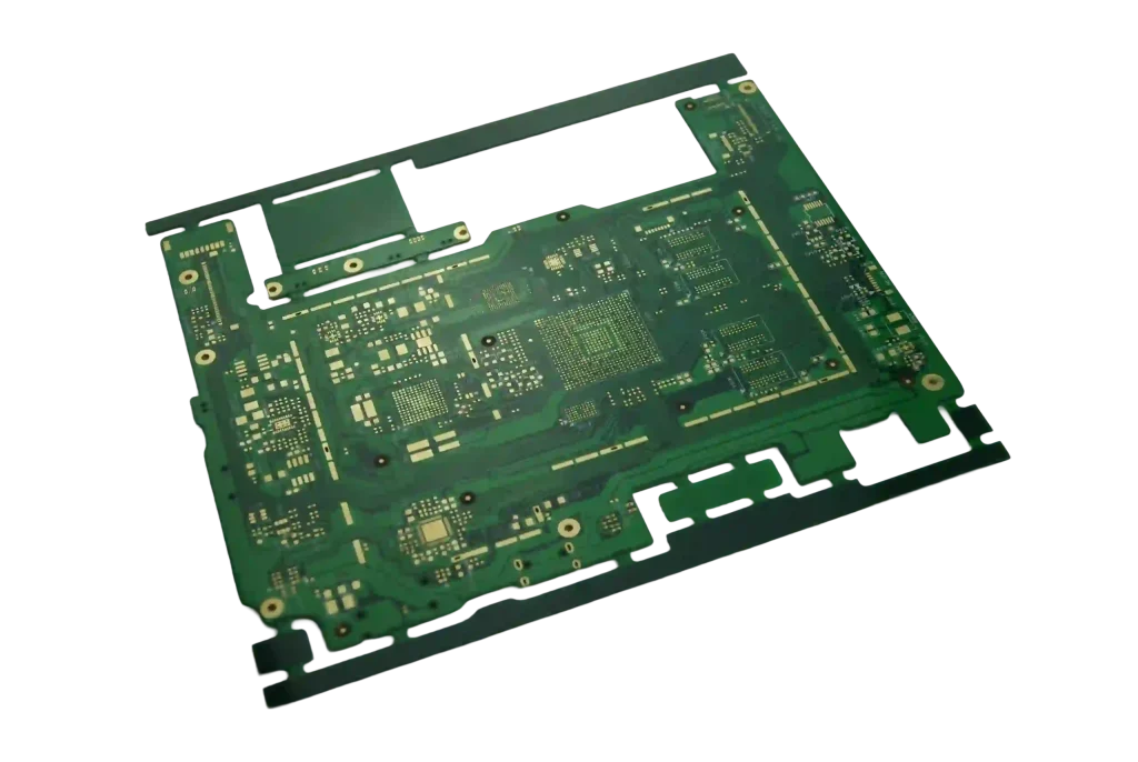
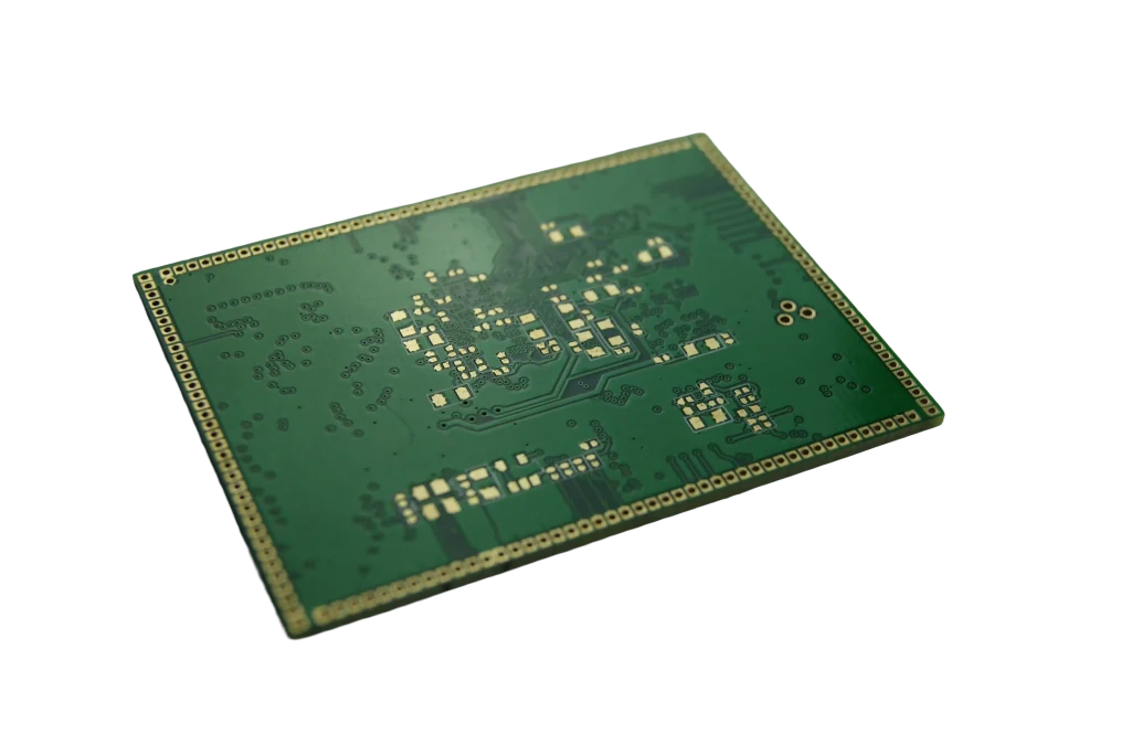
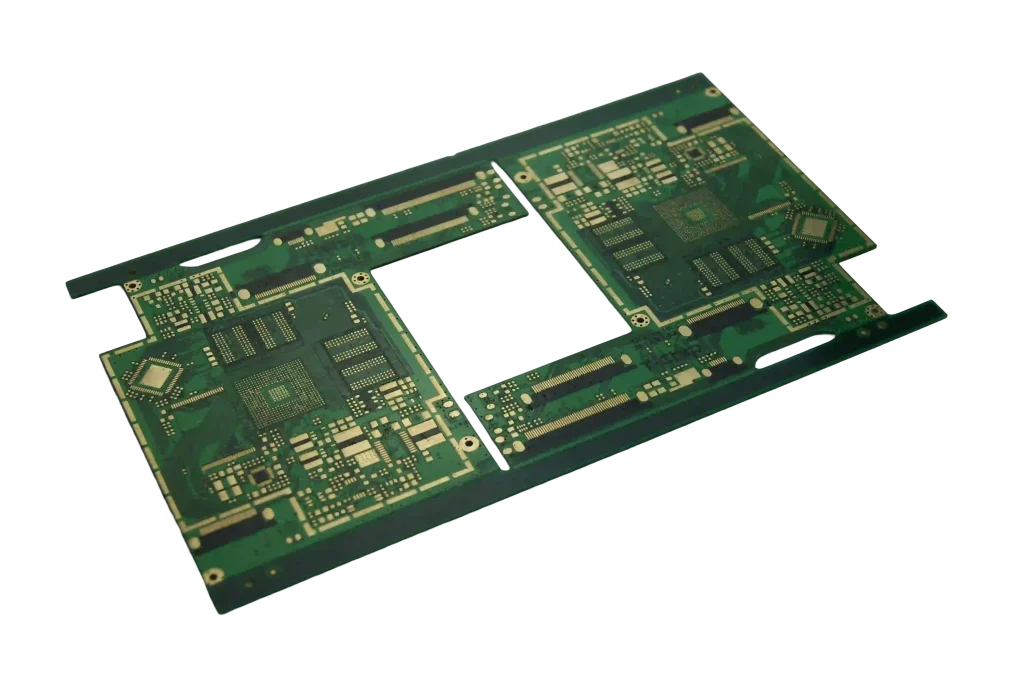
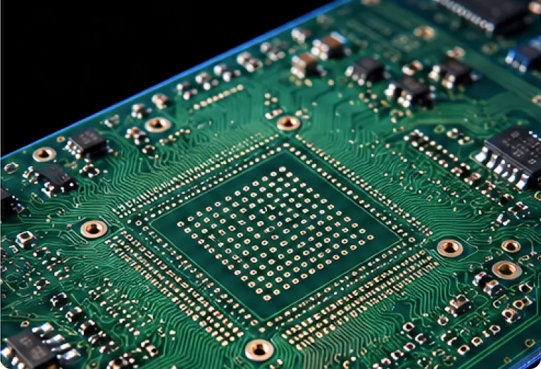
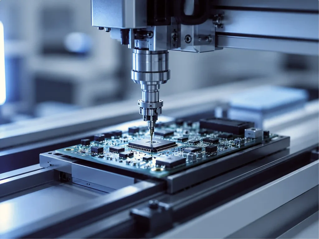
Leading High-Speed PCB Precision Manufacturing delivers controlled impedance boards with low signal loss, stable transmission performance, and reliable fabrication for high-frequency electronic applications.
High-Speed PCB Manufacturing Advantage delivers stable impedance control, low signal loss, and precise fabrication processes to ensure reliable high-frequency performance for advanced electronic systems.
In-house Integration
In-house Integration enables complete control over high-speed PCB fabrication, from material preparation and impedance management to testing and inspection, ensuring consistent quality, faster delivery, and stable signal performance.
End-to-end process control
Stable impedance consistency
Faster production cycles
Reduced supply chain risks
Reliable quality assurance
Advanced Equipment
Advanced Equipment supports high-speed PCB manufacturing with precision imaging, controlled impedance processes, and automated inspection systems, ensuring stable signal integrity and consistent production quality.
High-precision imaging systems
Controlled impedance process tools
Automated optical inspection
Advanced drilling equipment
Real-time process monitoring
Extensive RF/Microwave Materials Library
Extensive RF/Microwave Materials Library supports high-speed PCB manufacturing with low-loss laminates, stable dielectric performance, and reliable signal transmission for demanding RF and microwave applications.
Low-loss RF laminates available
Stable dielectric constant control
High-frequency signal support
Wide material selection range
Proven microwave performance
Production Excellence
Advanced High-Speed PCB Production Excellence
Advanced High-Speed PCB Production Excellence ensures precise impedance control, low signal loss, and stable multilayer fabrication for reliable high-frequency performance in demanding electronic applications.
Signal Restoration
Signal Restoration improves high-speed PCB performance by reducing distortion and maintaining clean signal integrity.
01
Impedance Control
Impedance Control ensures stable signal transmission in high-speed PCB by maintaining precise trace geometry.
02
Precision Back Drilling
Precision Back Drilling removes via stubs in high-speed PCB to improve signal integrity and reduce reflection loss.
03
Fine Etching
Fine Etching ensures precise trace definition in high-speed PCB, supporting stable impedance and low signal loss.
04
Manufacturing Capability
High-Speed PCB Manufacturing Capability
High-Speed PCB Manufacturing Capability covers multilayer fabrication, controlled impedance design, and precision processing to support stable high-frequency performance in advanced electronic applications.
Quality Control of High-Speed PCB ensures strict inspection of impedance, signal integrity, and layer alignment through AOI, X-ray, and electrical testing for reliable high-frequency performance.
Quality Control Equipment
Quality Control Equipment for High-Speed PCB includes AOI, X-ray inspection, and flying probe testing systems to ensure precise defect detection and stable signal integrity throughout production.
TDR Testing
TDR testing is used in high-speed PCB quality control to verify impedance consistency, detect signal discontinuities, and ensure stable transmission performance across high-frequency circuits.
Vector Network Analysis
Vector Network Analysis (VNA) is applied in high-speed PCB testing to evaluate signal transmission characteristics, ensuring accurate impedance control, low loss, and stable high-frequency performance.
Automated Optical Inspection
Automated Optical Inspection (AOI) is used in high-speed PCB production to detect surface defects, misalignment, and pattern issues, ensuring consistent quality and reliable manufacturing output.
X-ray Inspection
X-ray inspection is applied in high-speed PCB manufacturing to verify internal structures such as vias and solder joints, ensuring hidden defects are detected and product reliability is maintained.
Quality Control Equipment
Quality Standard Certificates ensure High-Speed PCB manufacturing complies with international standards such as ISO, IPC, and RoHS, guaranteeing process stability, material traceability, and consistent high-frequency performance for global applications.
IS0 9001:2015
stepping stone
The most fundamental and universally applicable quality management systemcertification.
IPC A 610
Industry Standard
The most authoritative international standard for the acceptance of electronic assembly and PCB manufacturing.
IATF 16949:2016
Automotive-grade (high gold content)
Demonstrate the capability to manufacture highly reliable automotive PCB.
ISO 13485
Medical-grade (high gold content)
Demonstrate the capability to manufacture high-precision PCB for medical equipment.
ISO14001:2015
Environmental system
Green factory certification is highly valued by major manufacturers and overseas clients.
UL
Safety Certification
Mandatory safety and flame-retardant standards for entering the North American market.
RoHS
Environmental regulations
Restriction of Hazardous Substances (RoHS) Directive (a standard requirement for electronic products exported to the EU).
REACH
Environmental regulations
EU Regulation on the Registration, Evaluation, Authorisation and Restriction of Chemicals.
IS0 9001:2015
01
IPC A 610
02
IATF 16949:2016
03
ISO 13485
04
ISO14001:2015
05
UL
06
RoHS
07
REACH
08
Applications
High-Speed PCB Application
High-Speed PCB Application includes communication systems, automotive electronics, industrial control, and computing devices, delivering stable signal integrity and reliable high-frequency performance.
01
Telecom Systems
02
Automotive Electronics
03
Computing Platforms
04
Medical Devices
05
Industrial Control
01
Telecom Systems
High-Speed PCB applications in telecom systems support stable signal transmission, controlled impedance routing, and low-loss performance for base stations, networking equipment, and high-frequency communication modules.
02
Automotive Electronics
High-Speed PCB applications in automotive electronics ensure reliable operation for ADAS, radar, and infotainment systems, delivering robust signal integrity under high-temperature and high-vibration conditions.
03
Computing Platforms
High-Speed PCB applications in computing platforms enable high-bandwidth data transfer, low signal distortion, and optimized thermal performance for servers, processors, and advanced computing hardware.
04
Medical Devices
High-Speed PCB applications in medical devices ensure precise signal integrity and reliability for imaging systems, diagnostic equipment, and patient monitoring devices requiring stable high-frequency performance.
05
Industrial Control
High-Speed PCB applications in industrial control systems provide stable data transmission and noise resistance, supporting PLCs, automation modules, and precision control equipment in demanding environments.
FAQ
High-Speed PCB FAQ
High-Speed PCB FAQ provides clear answers on impedance control, material selection, design rules, and manufacturing processes to help ensure reliable signal integrity and stable high-frequency performance.
Q1
What materials are used for High-Speed PCB manufacturing?
High-Speed PCB typically use low-loss laminates such as Rogers, Megtron, and high-Tg FR4 to ensure stable dielectric performance and signal integrity.
Q2
How is impedance control achieved in High-Speed PCB?
Impedance control is achieved through precise stack-up design, accurate trace geometry, and strict process control during fabrication to maintain consistent signal performance.
Q3
What testing methods are used for High-Speed PCB?
High-Speed PCB are tested using TDR, VNA, AOI, X-ray, and electrical testing to verify signal integrity, structural accuracy, and manufacturing reliability.
Q4
What industries commonly use High-Speed PCB?
High-Speed PCB are widely used in telecom, automotive electronics, industrial automation, computing systems, and advanced medical devices requiring stable high-frequency performance.
Solutions
High-Speed PCB Solutions
High-Speed PCB Solutions deliver controlled impedance, low-loss materials, and precise fabrication processes for reliable signal integrity in telecom, automotive, industrial, and computing applications.
LT CIRCUIT Knowledge Base delivers practical PCB and PCBA knowledge, covering fabrication processes, assembly techniques, materials, and quality control for better engineering decisions.