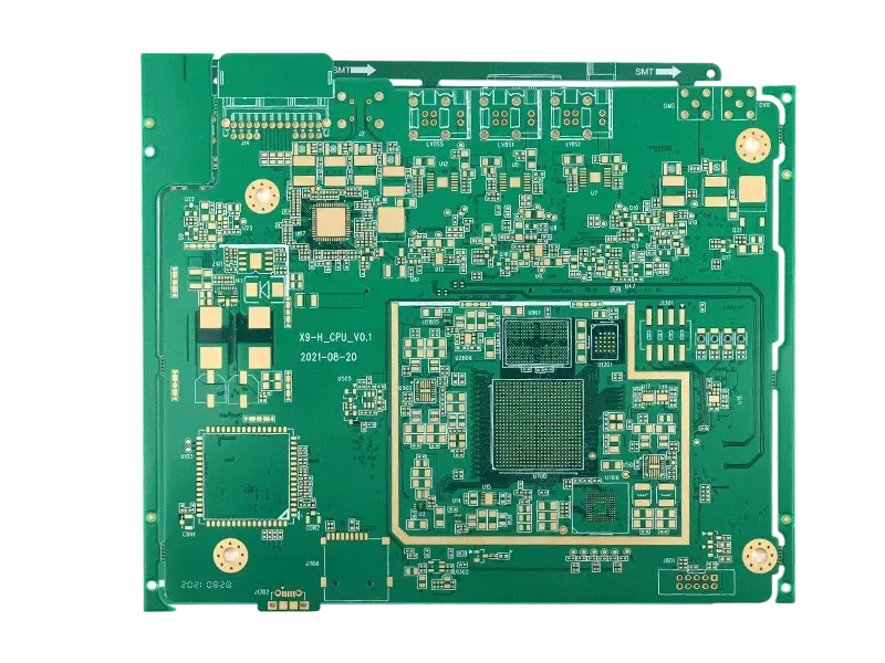
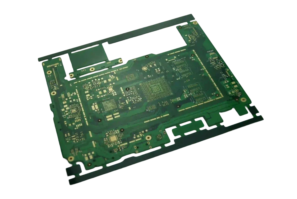
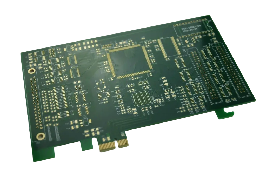
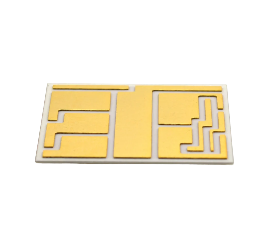
High-Precision PCB Manufacturing in EMS Industry provides reliable fabrication for multilayer, HDI, and high-frequency boards, ensuring stable performance, tight tolerance control, and consistent quality for complex electronic applications.
The PCB Manufacturing Process covers material selection, imaging, etching, drilling, plating, and final testing to ensure high precision, stable performance, and reliable quality for advanced electronic applications.
Laser Drilling Process
Laser drilling enables precise microvia formation for HDI PCB, ensuring high accuracy, fine interconnection, and stable signal performance in advanced multilayer designs used in compact electronic applications.
Laser Imaging Process
Laser imaging ensures high-resolution pattern transfer on PCB layers, improving line definition, registration accuracy, and consistency for high-density and high-performance circuit manufacturing.
Electroplating Process
Electroplating builds reliable copper thickness in vias and traces, ensuring excellent conductivity, mechanical strength, and stable electrical performance across multilayer PCB structures.
Etching Process
Etching removes unwanted copper with controlled precision, forming accurate circuit patterns while maintaining edge quality, dimensional stability, and consistent electrical performance.
Transforming Customer Designs into Market-ready Products Through High-precision Hardware and Advanced Manufacturing Processes.
We transform customer PCB designs into market-ready products through high-precision fabrication, advanced process control, and strict quality systems, ensuring reliable performance and consistent manufacturing output.
Our advanced manufacturing processes convert complex electronic designs into stable, high-quality PCB with optimized materials, precise engineering, and scalable production for global industrial applications.
Product Showcase
PCB Product Gallery
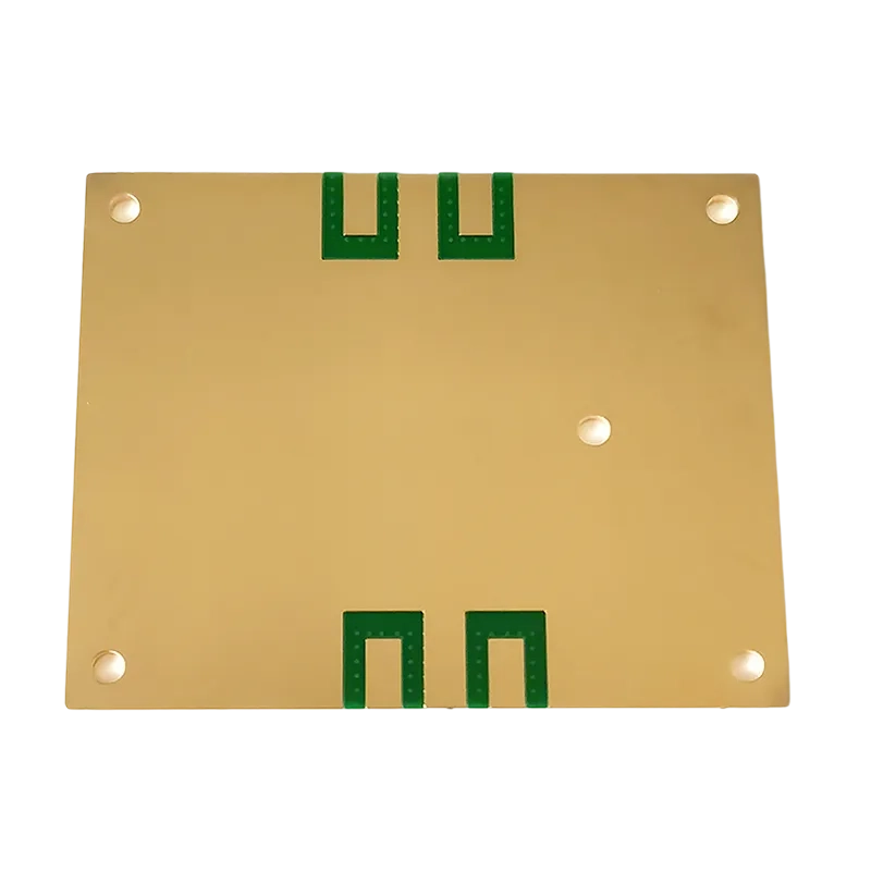
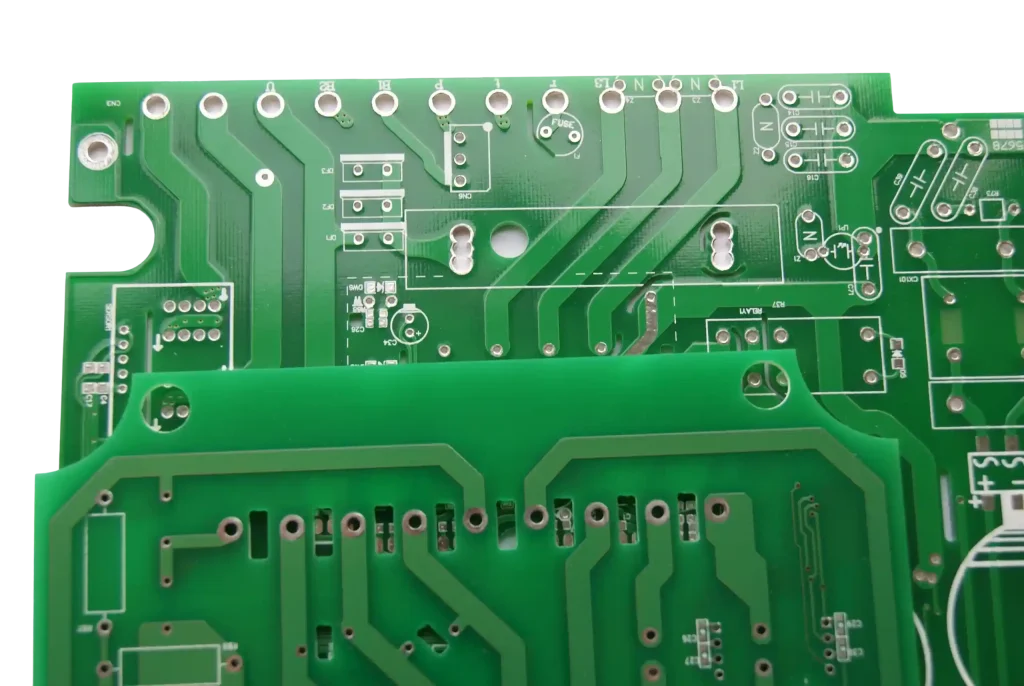
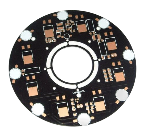
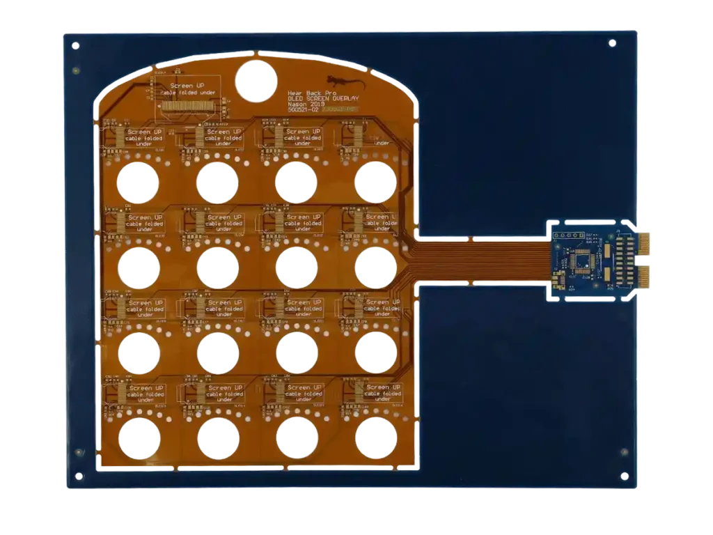
The PCB Product Gallery showcases high-precision multilayer, HDI, high-frequency, and power PCB solutions designed for industrial, automotive, communication, and advanced electronic applications worldwide.
Metal-based PCB
HDI-3
High speed PCB
Ceramic PCB
High speed PCB
Thick copper PCB
Rogers PCB
CONTACT US FOR EXPERT CONSULTATION
Let us know your requirement. We will connect best products with you.