Advantages

HDI PCB Manufacturing Advantage

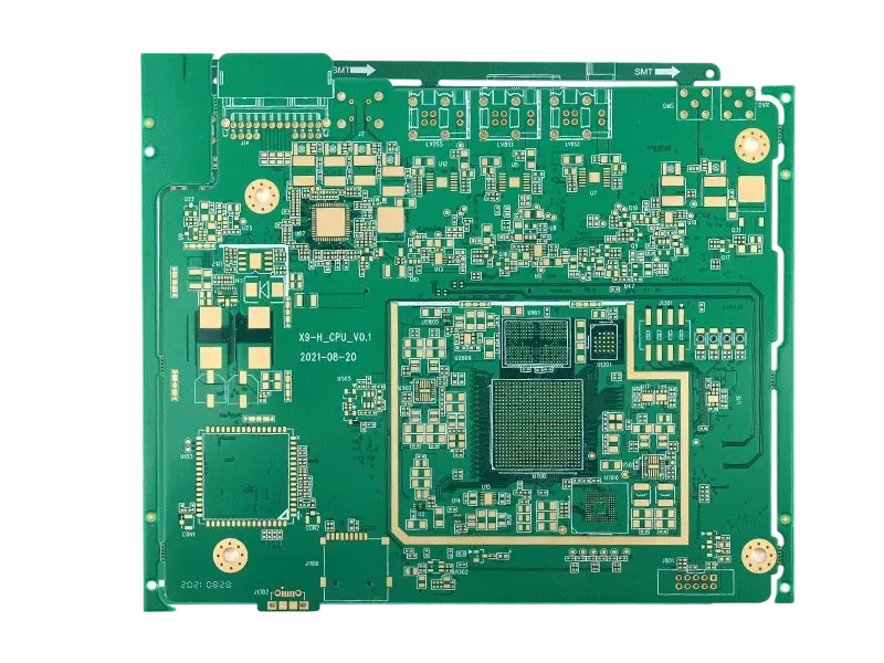
HDI PCB Manufacturing Advantage enables finer traces, laser microvias, and higher wiring density, providing enhanced electrical performance and space-saving solutions for advanced electronic applications.

In-house Integration

In-house Integration enables complete control over HDI PCB production, from laser drilling and imaging to plating and testing, ensuring consistent quality, shorter lead times, and improved manufacturing efficiency.

End-to-end process control

Faster production turnaround

Stable quality consistency

Reduced outsourcing risks

Enhanced manufacturing efficiency

Advanced Equipment

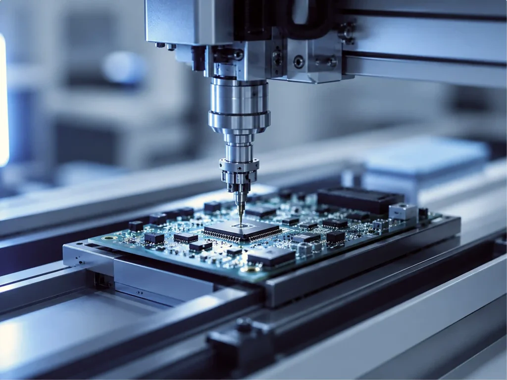
Advanced Equipment supports high-precision HDI PCB manufacturing with laser drilling, direct imaging, and automated inspection systems, ensuring excellent registration accuracy, stable process control, and reliable performance for complex multilayer designs.
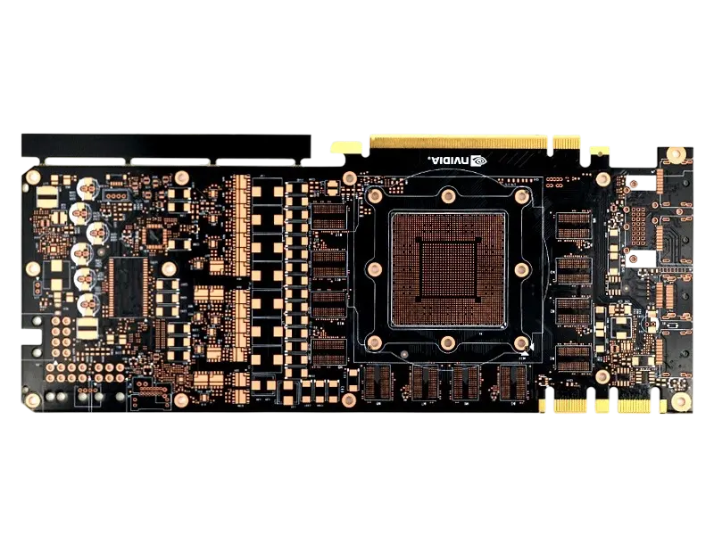
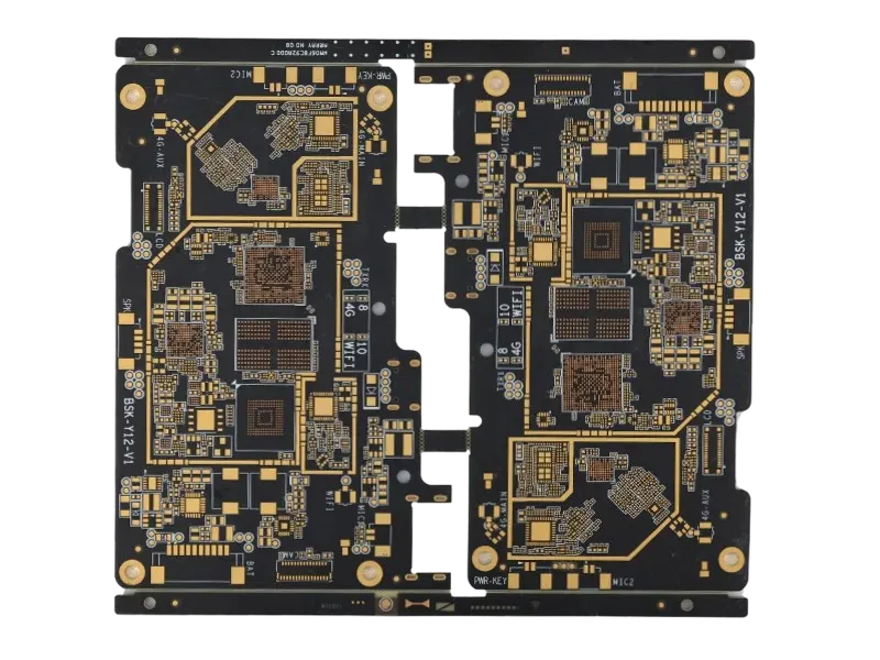
Laser microvia drilling systems

Direct imaging technology

Automated process control

High-precision layer alignment

Advanced inspection equipment

High-Mix, Low-Volume

High-Mix, Low-Volume manufacturing provides flexible HDI PCB production for prototypes and diverse product requirements, enabling rapid changeovers, stable quality, and efficient support for complex and customized electronic applications.

Flexible production scheduling

Fast prototype support

Multiple product configurations

Efficient changeover capability

Consistent quality performance

Production Excellence

Advanced HDI PCB Production Excellence

Advanced HDI PCB Production Excellence delivers superior interconnection density, precise microvia structures, and stable manufacturing quality for high-performance electronic applications.

Laser Drilling

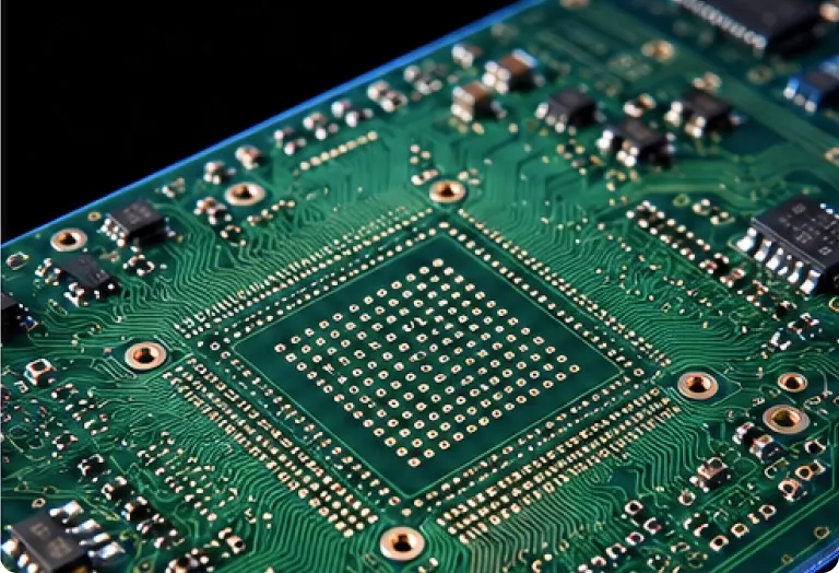
Laser drilling enables accurate microvia formation for HDI PCB, supporting fine-pitch and compact designs.

01

Sequential Lamination

Sequential lamination supports multilayer HDI designs with accurate layer buildup and stable performance.

02

Through-hole Plating

Through-hole plating provides stable copper coverage for dependable conductivity and interconnection.

03

Fine Etching

Fine etching enables precise circuit definition for HDI boards with fine lines and high density.

04

Advanced HDI PCB Production Excellence

Manufacturing Capability

HDI PCB Manufacturing Capability

The Production Capacity Table presents essential HDI PCB specifications, covering layer structures, fine-line capability, laser microvias, and process tolerances for advanced electronic applications.

Item

Capability

Layer Count

4–64 Layers

Board Thickness

0.2–3.2 mm

Copper Thickness

0.5–10oz

Surface Finish

ENIG, OSP, Immersion Silver

Impedance Control Tolerance

>±5%

Registration Accuracy

±25 μm

IPC Standard

IPC Class 2 / Class 3

Item

Capability

HDI Type

1+N+1, 2+N+2, 3+N+3

Sequential Lamination

Up to 6 Times

Laser Via Diameter

0.075 mm

Laser Pad Size

0.175 mm

Via Capture Pad

0.225 mm

Min Trace Width/Space

2/2 mil

Via-in-Pad

Filled & Capped

Stacked Microvias

Available,》6 Times

Staggered Microvias

Available

Copper Filling Process

Available,0.15 mm < Hole Diameter ≤ 3.0 mm

Resin Plugging

Available,0.2 mm < Hole Diameter ≤ 0.6 mm

Any-Layer HDI

Available

AOI Inspection

100%

X-ray Alignment

Available

The table above only lists process parameters for HDI PCB products. Please download the full process manual.

Quality Control

Quality Control of HDI PCB

Quality Control of HDI PCB applies strict process monitoring, AOI, and electrical testing to ensure precision, reliability, and consistent manufacturing quality.

Quality Control Equipment

Quality Control Equipment integrates AOI systems, X-ray inspection, and flying probe testing to ensure precise defect detection and consistent HDI PCB manufacturing quality.

AOI Inspection Systems

AOI inspection systems enable real-time defect detection on HDI PCB, ensuring accurate solder joints, trace integrity, and consistent quality throughout high-density production processes.

X-Ray Inspection Equipment

X-ray inspection equipment verifies hidden solder joints and microvia structures, ensuring internal connection reliability and detecting defects in complex HDI PCB assemblies.

Flying Probe Testing

Flying probe testing provides flexible electrical verification for HDI PCB, ensuring circuit continuity, insulation performance, and stable functionality without custom fixtures.

Automated Electrical Testing

Automated electrical testing systems validate HDI PCB performance, detecting opens, shorts, and resistance issues to ensure reliable operation in advanced electronic applications.

Quality Control Equipment

The Production Capacity Table presents essential HDI PCB specifications, covering layer structures, fine-line capability, laser microvias, and process tolerances for advanced electronic applications.

IS0 9001:2015

stepping stone

The most fundamental and universally applicable quality management systemcertification.

IPC A 610

Industry Standard

The most authoritative international standard for the acceptance of electronic assembly and PCB manufacturing.

IATF 16949:2016

Automotive-grade (high gold content)

Demonstrate the capability to manufacture highly reliable automotive PCB.

ISO 13485

Medical-grade (high gold content)

Demonstrate the capability to manufacture high-precision PCB for medical equipment.

ISO14001:2015

Environmental system

Green factory certification is highly valued by major manufacturers and overseas clients.

UL

Safety Certification

Mandatory safety and flame-retardant standards for entering the North American market.

RoHS

Environmental regulations

Restriction of Hazardous Substances (RoHS) Directive (a standard requirement for electronic products exported to the EU).

REACH

Environmental regulations

EU Regulation on the Registration, Evaluation, Authorisation and Restriction of Chemicals.

certifications-info

IS0 9001:2015

01

IPC A 610

02

IATF 16949:2016

03

ISO 13485

04

ISO14001:2015

05

UL

06

RoHS

07

REACH

08

Applications

HDI PCB Application

HDI PCB Application supports compact and high-performance electronic products, widely used in mobile devices, automotive electronics, industrial systems, and advanced communication equipment.

01

Smart Devices

02

Automotive Electronics

03

Communication Equipment

04

Medical Electronics

05

Industrial Control

01

Smart Devices

HDI PCB are widely used in smartphones, wearables, and smart home devices, enabling compact designs, high-speed signal transmission, and reliable performance for modern consumer electronics.

02

Automotive Electronics

HDI PCB applications in automotive systems support ADAS, infotainment, and control units, delivering stable performance, high reliability, and resistance to harsh environmental conditions.

03

Communication Equipment

HDI PCB are essential for communication devices such as base stations and network modules, ensuring high-frequency performance, signal integrity, and dense interconnection capability.

04

Medical Electronics

HDI PCB support advanced medical devices, offering high precision, reliability, and miniaturization for diagnostic, monitoring, and life-support electronic systems.

05

Industrial Control

HDI PCB applications in industrial control systems provide stable operation, high durability, and precise signal processing for automation, robotics, and intelligent manufacturing equipment.

FAQ

HDI PCB FAQ

HDI PCB FAQ explains common questions about stack-up design, microvia technology, materials, tolerances, and testing standards to support efficient engineering communication.

Q1

What is the typical layer count for HDI PCB production?

HDI PCB typically range from 4 to 12 layers, depending on design complexity and application requirements, with support for sequential lamination structures.

Q2

What microvia technologies are used in HDI PCB?

Laser-drilled microvias, blind vias, and buried vias are commonly used to achieve high-density interconnection and improved signal performance.

Q3

What materials are suitable for HDI PCB manufacturing?

Standard FR4, high-Tg materials, and low-loss laminates are used based on electrical performance, thermal requirements, and application environments.

Q4

What quality testing is applied to HDI PCB?

HDI PCB undergo AOI inspection, X-ray analysis, electrical testing, and reliability validation to ensure consistent quality and defect-free production.

Solutions

HDI PCB Solutions

HDI PCB Solutions provide high-density routing, laser microvia technology, and multilayer integration for demanding applications in automotive, communication, medical, and consumer electronics.

PCB Manufacturing Capabilities-2

Title of the Article Details Page

h2 Add Your Heading Text Here Advanced battery systems maximize energy utilization by efficiently storing and distributing power, reducing energy waste and improving overall performance.Advanced battery systems maximize energy utilization by efficiently storing and distributing power, reducing energy waste and improving overall performance.Advanced battery systems maximize energy utilization by efficiently storing and distributing power, reducing […]

Read More

LT CIRCUIT EMS Multimedia Center

Title of the Article Details Page

Read More

Aerospace PCB Application Showcase-1

Title of the Article Details Page

Read More

Contact Our Team

LT CIRCUIT Knowledge Base delivers practical PCB and PCBA knowledge, covering fabrication processes, assembly techniques, materials, and quality control for better engineering decisions.

*We respect your confidentiality and all information is protected.

CONTACT US FOR EXPERT CONSULTATION

Let us know your requirement. We will connect best products with you.

*We respect your confidentiality and all information is protected.

Download Now

Complete the form below to access your download instantly.

*We respect your confidentiality and all information is protected.