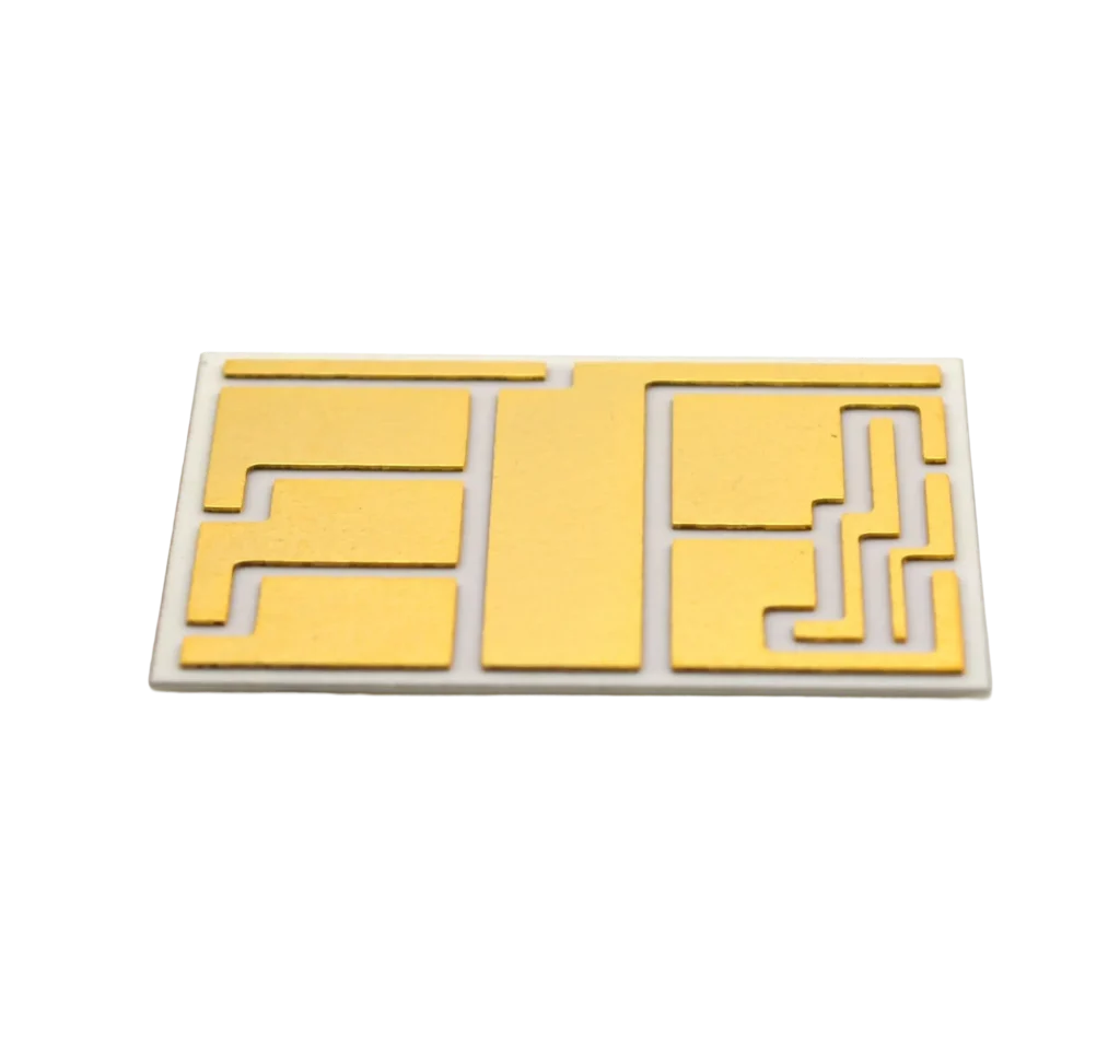
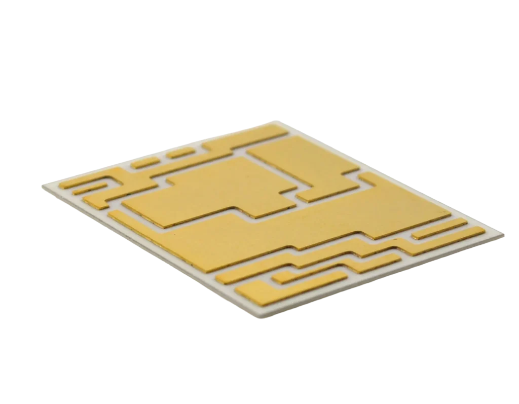
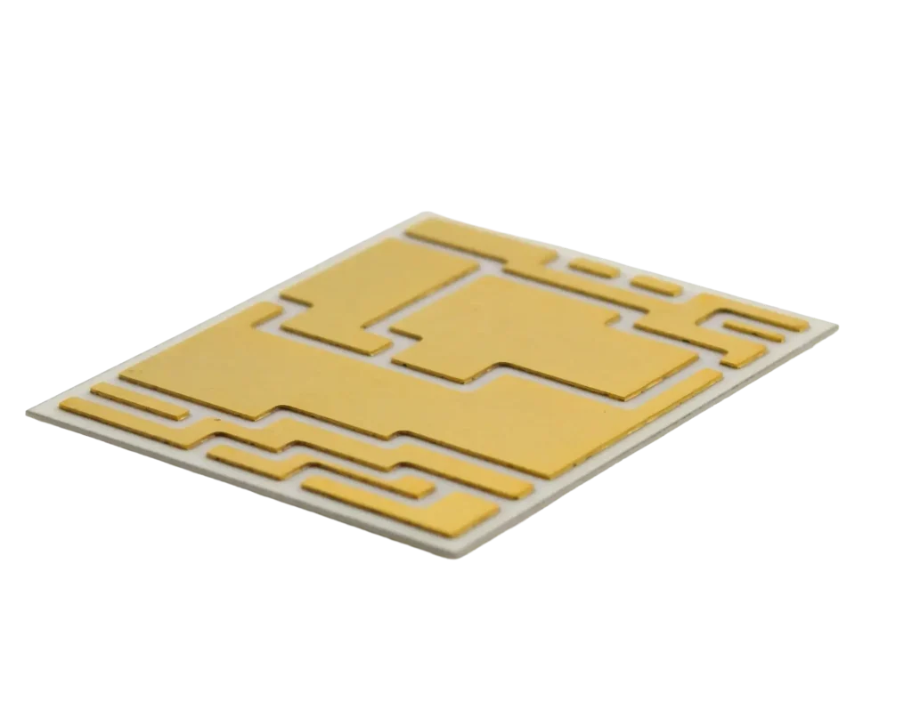
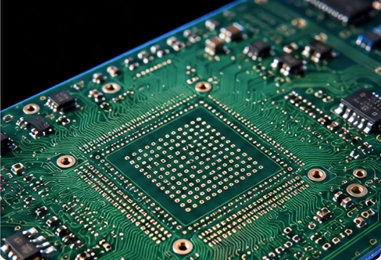
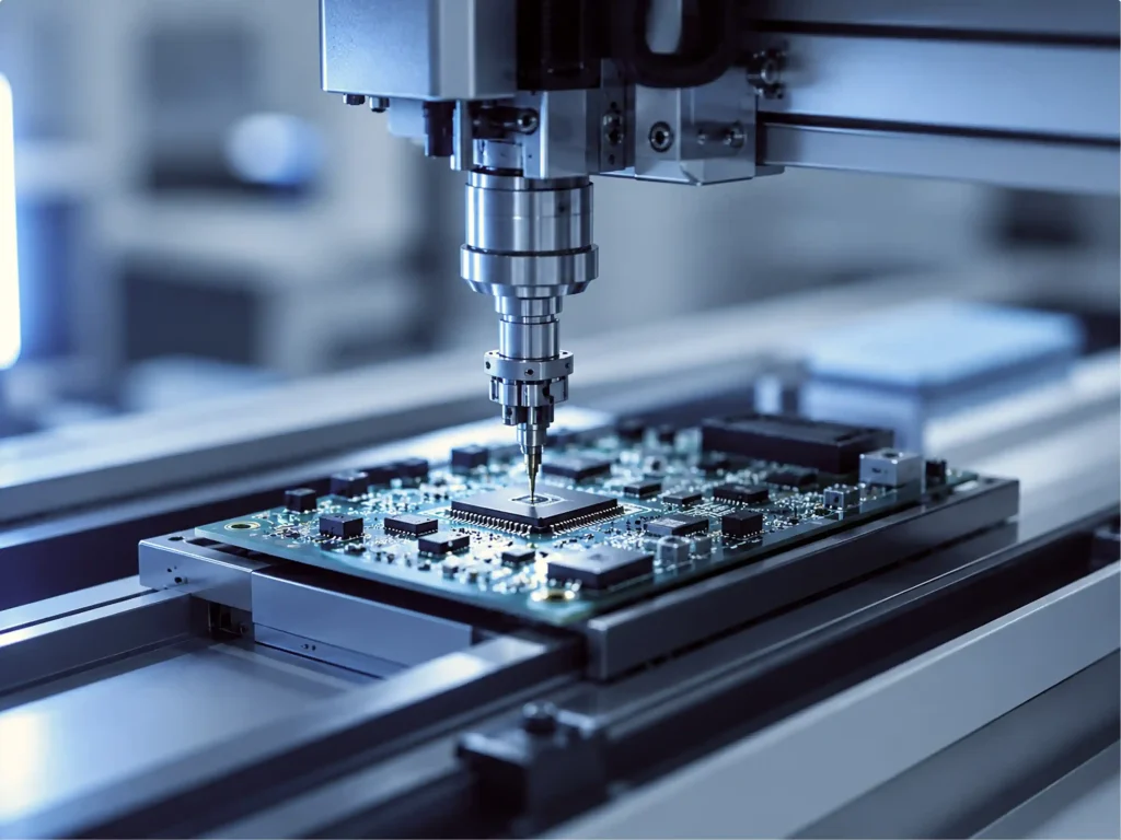
Leading Ceramic PCB Precision Manufacturing delivers high thermal conductivity, stable dielectric performance, and reliable circuit integration for high-power and high-frequency electronic applications.
Ceramic PCB Manufacturing Advantage ensures superior thermal conductivity, high insulation stability, and precise circuit formation for demanding high-power and high-frequency electronic applications.
Thermal Management Expert
Thermal Management Expert in ceramic PCB manufacturing ensures efficient heat dissipation, stable thermal performance, and reliable operation for high-power and high-frequency electronic applications.
Efficient heat dissipation control
Stable thermal performance design
High-power application support
Reliable thermal conductivity
Enhanced system durability
In-house Assurance
In-house Assurance for ceramic PCB manufacturing ensures full process control from material selection to final inspection, delivering consistent quality, stable performance, and reliable production outcomes.
Full process quality control
Stable production consistency
Strict material verification
Integrated manufacturing flow
Reliable delivery assurance
Fast-turn Delivery
Fast-turn Delivery in ceramic PCB manufacturing enables rapid prototyping and efficient production scheduling while maintaining strict quality control and stable high-performance output for urgent applications.
Rapid prototype support
Short lead time production
Flexible scheduling capability
Stable quality assurance
Efficient order processing
Production Excellence
Advanced Ceramic PCB Production Excellence
Advanced Ceramic PCB Production Excellence delivers precise metallization, stable high-temperature performance, and reliable interconnection for demanding high-power and RF electronic applications.
Precision Cutting
Precision Cutting ensures accurate ceramic PCB shaping with smooth edges and stable structural integrity.
01
Laser Drilling
Laser Drilling enables precise micro-hole formation in ceramic PCB for high-density and reliable interconnection.
02
Vacuum Coating
Vacuum Coating provides uniform metal deposition on ceramic PCB ensuring stable conductivity and reliability.
03
Pattern Plating
Pattern Plating enables precise circuit formation on ceramic PCB ensuring stable conductivity and fine line accuracy.
04
Manufacturing Capability
Ceramic PCB Manufacturing Capability
Our ceramic PCB manufacturing capability covers precision machining, fine circuit fabrication, and reliable metallization to support demanding thermal and electrical performance requirements.
Item
Capability
Layer Count
1–8 Layers
Board Thickness
0.25–3.0 mm
Ceramic Thickness
0.10–1.50 mm
Copper Thickness
0.5–10 oz
Min Trace Width/Space
3/3 mil
Min Hole Size
0.10 mm
Hole Tolerance
±0.05 mm
Panel Size
Max. 300 × 300 mm
Surface Finish
ENIG, Immersion Silver, OSP
IPC Standard
IPC Class 2 / Class 3
UL Certification
Available
RoHS & REACH Compliance
Yes
Item
Capability
Ceramic Material Type
Alumina, Aluminum Nitride, Silicon Nitride
Manufacturing Process
DBC, DPC, AMB, Thick Film
Maximum Copper Thickness
10 oz
Minimum Line Width/Spacing
2/2 mil
Laser Drilling
Available
Metallized Via
Available
Filled Via
Available
Blind Via Structure
Available
Double-Sided Metallization
Available
Gold Plating
Available
Silver Plating
Available
Copper Coin Technology
Available
High Thermal Conductivity Design
Available
Hybrid Ceramic Construction
Available
Hermetic Packaging Structure
Available
High Voltage Isolation
Available
High Current Design
Available
The table above only lists process parameters for HDI PCB products. Please download the full process manual.
Quality Control of Ceramic PCB ensures strict inspection of thermal performance, dimensional accuracy, and metallization quality using AOI, X-ray, and electrical testing for stable and reliable operation.
Quality Control Equipment
Quality Control Equipment for Ceramic PCB includes AOI systems, X-ray inspection, and high-precision metrology tools to ensure dimensional accuracy, metallization quality, and stable electrical performance.
TDR Testing
TDR testing is applied in ceramic PCB quality control to verify impedance consistency, detect signal discontinuities, and ensure stable high-frequency electrical performance across critical circuits.
High-Frequency Test
Vector Network Analyzer (VNA) testing verifies impedance accuracy, insertion loss, and return loss to ensure ceramic PCB deliver stable RF performance and dependable signal integrity.
Automated Optical Inspection
Automated Optical Inspection (AOI) is used in ceramic PCB production to detect surface defects, pattern deviations, and alignment issues, ensuring consistent quality and reliable circuit performance.
X-ray Inspection
X-ray inspection is applied in ceramic PCB quality control to verify internal structures, detect hidden defects, and ensure reliable metallization and stable electrical performance.
Quality Control Equipment
Quality Standard Certificates ensure Ceramic PCB manufacturing complies with ISO, IPC, and RoHS requirements, guaranteeing process stability, material traceability, and consistent thermal and electrical performance for global applications.
IS0 9001:2015
stepping stone
The most fundamental and universally applicable quality management systemcertification.
IPC A 610
Industry Standard
The most authoritative international standard for the acceptance of electronic assembly and PCB manufacturing.
IATF 16949:2016
Automotive-grade (high gold content)
Demonstrate the capability to manufacture highly reliable automotive PCB.
ISO 13485
Medical-grade (high gold content)
Demonstrate the capability to manufacture high-precision PCB for medical equipment.
ISO14001:2015
Environmental system
Green factory certification is highly valued by major manufacturers and overseas clients.
UL
Safety Certification
Mandatory safety and flame-retardant standards for entering the North American market.
RoHS
Environmental regulations
Restriction of Hazardous Substances (RoHS) Directive (a standard requirement for electronic products exported to the EU).
REACH
Environmental regulations
EU Regulation on the Registration, Evaluation, Authorisation and Restriction of Chemicals.
IS0 9001:2015
01
IPC A 610
02
IATF 16949:2016
03
ISO 13485
04
ISO14001:2015
05
UL
06
RoHS
07
REACH
08
Applications
Ceramic PCB Application
Ceramic PCB Application includes power electronics, RF and microwave systems, automotive modules, industrial control, and medical devices, delivering stable thermal and electrical performance.
01
Power Electronics
02
Automotive Electronics
03
RF & Microwave Systems
04
Medical Devices
05
Industrial Control
01
Power Electronics
Ceramic PCB applications in power electronics deliver excellent thermal conductivity, stable insulation, and reliable performance for high-power modules, converters, and energy control systems.
02
Automotive Electronics
Ceramic PCB applications in automotive electronics provide high thermal resistance and stable electrical performance for engine control, power modules, and advanced driver assistance systems.
03
RF & Microwave Systems
Ceramic PCB applications in RF and microwave systems ensure low dielectric loss, stable signal transmission, and high-frequency performance for communication and radar-related electronic devices.
04
Medical Devices
Ceramic PCB applications in medical devices ensure high reliability, precise signal integrity, and stable thermal performance for imaging systems, diagnostic equipment, and monitoring devices.
05
Industrial Control
Ceramic PCB applications in industrial control support reliable operation in harsh environments, ensuring stable signal processing, durability, and long-term system performance for automation equipment.
FAQ
Ceramic PCB FAQ
Ceramic PCB FAQ provides answers on material selection, thermal performance, manufacturing process, tolerances, and testing methods to support engineering design and production decisions.
Q1
What materials are used in Ceramic PCB manufacturing?
Ceramic PCB are typically made from alumina, aluminum nitride, or other high-performance ceramic substrates selected for thermal conductivity and electrical stability.
Q2
What are the key advantages of Ceramic PCB?
Ceramic PCB offer excellent thermal management, high insulation performance, and stable operation in high-power and high-frequency environments.
Q3
How is quality ensured in Ceramic PCB production?
Quality is ensured through strict process control, AOI, X-ray inspection, and electrical testing covering metallization, dimensional accuracy, and thermal performance.
Q4
What applications commonly use Ceramic PCB?
Ceramic PCB are widely used in power electronics, RF/microwave systems, automotive modules, industrial control, and medical devices requiring high reliability.
Solutions
Ceramic PCB Solutions
Ceramic PCB Solutions provide high thermal conductivity substrates, precise circuit fabrication, and reliable performance for power electronics, RF systems, automotive modules, and industrial applications.
LT CIRCUIT Knowledge Base delivers practical PCB and PCBA knowledge, covering fabrication processes, assembly techniques, materials, and quality control for better engineering decisions.